
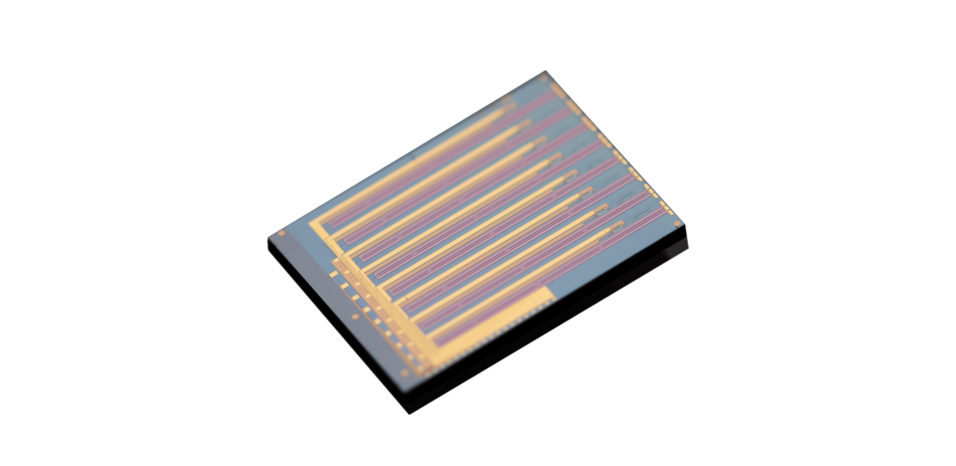
Material properties enter a network through several translations. Electro-optic response shapes the waveguide and electrode; the die then meets a package, driver, and link. The place of tfln chips lies at the device stage of that chain.
The electro-optic effect links an applied field to a change in refractive index. Optical transparency and material quality shape the starting conditions, while fabrication determines propagation loss and dimensional control. The governing factors create design options; they do not determine the response of a packaged modulator.
Electrical and optical paths then translate the material into a working circuit. Interaction length, electrode spacing, impedance, microwave loss, optical confinement, and termination influence the trade between bandwidth and drive. Fiber attachment and radio-frequency launches can further change what a customer measures at external connectors.
A business assessment of tfln chips follows the chain from property to design and finally to system impact. The relevant questions concern repeatability, interface ownership, test conditions, volume readiness, and whether the device reduces cost or power within the customer’s actual assembly.
Documentation should preserve that chain. Material certificates, fabrication maps, device measurements, package identifiers, and final test data help a later failure to be traced and separates material effects from other performance changes. Traceability also supports controlled process or supplier revisions.
Material Properties Shape Electro-Optic Response
For photonic chips made on thin-film lithium niobate, electro-optic response provides a mechanism for changing optical phase or intensity with an electrical signal. The strength of that mechanism is considered with film quality, crystal orientation, optical wavelength, and the field distribution produced by the electrodes.
Material loss sets only one part of the loss budget in photonic chips. Waveguide sidewalls, bends, splitters, couplers, transitions, and package interfaces typically contribute additional penalties. A supplier comparison identifies where each quoted loss is measured so chip-level and connectorized results are not treated as equivalent.
Transparency range and optical power handling potentially affect application fit, yet final limits depend on circuit and package details. Engineering teams should request conditions, sample count, and environmental state for any reported result. General material descriptions are useful for screening but insufficient for component approval.
Process variation modifies the physical starting point. Film thickness, surface condition, etch depth, and dimensional bias typically shift optical confinement or electrode interaction across the fabricated area. Statistical evidence therefore matters when a customer intends to move from development quantities to repeatable production.
Waveguide and Electrode Design Convert Potential into Devices
Waveguide geometry controls optical mode confinement, bend behavior, coupling, and sensitivity to fabrication variation. Strong confinement often enables compact routing, while tighter dimensions may increase process sensitivity. Designers must choose a geometry that fits performance and yield objectives with compactness balanced against production margin.
Electrodes have a separate but connected task. Impedance, microwave velocity, conductor loss, spacing, and termination influence how the drive signal travels beside the optical mode. Increasing interaction often improves modulation efficiency while adding radio-frequency loss or device length, so the optimum depends on the intended driver and baud rate.
Co-simulation becomes valuable because optical and electrical changes are not independent. A smaller gap may simultaneously alter efficiency, optical loss, process tolerance, and breakdown margin. Test structures can isolate these contributions before the complete circuit is committed.
Design margins are allocated to measured sources of variation. If electrode placement dominates response, tighter optical dimensions potentially add cost yet leaves yield unchanged. If coupling controls the link budget, effort belongs at the interface before further reductions in on-chip propagation loss.
Packaging preserves or degrades the designed response. Bonds, connectors, interposers, couplers, and thermal stress introduce new conditions. Customer-facing data should state whether measurements represent a bare die, probed chip, or packaged device so integration teams can build a realistic system model.
Chip Evaluation Through System-Level Trade-Offs
Device teams examine the TFLN chip configurations of Liobate through a property-to-system chain. The sourcing file for Liobate connects material certificates and fabrication-stage data with packaged response, driver power, optical margin, and lot consistency.
Specific product figures from the supplier retain their stated measurement conditions when they enter a design file. Project teams should confirm reference planes, sample form, drive method, and applicable configuration and limits each result to its measured chip or module configuration.
Risk review starts from the property-to-system chain for a TFLN chip. The program tracks material certificates, fabrication-stage data, package response, driver power, and link margin through pilot builds and ordinary operating conditions. Results for the property-to-system chain for a TFLN chip remain tied to the exact hardware, software, fixture, and process revision used to obtain them.
The final decision belongs to the complete link and manufacturing plan. Material properties explain why a TFLN approach is worth evaluating; verified device behavior and integration economics clarify whether it should be approved for a particular optical product.
Incoming inspection and final acceptance reuse the property-to-system chain established during development. Drift at the material, device, package, or driver level becomes visible before link failure.